Copper balance
A symmetric copper distribution (copper balance) on the circuit board is very important, because asymmetric copper leads to bow and twist effects.
This warping of the form is caused by thermal loads in the circuit board, such as those caused by the HAL manufacturing process (hot air leveling), or later during the assembly process (heat development in reflow, wave soldering, etc.), when asymmetrically arranged copper surfaces are present
"Bow" refers to a cylindrical or spherical deformation, in which the four corners of the circuit board lie in a single plane.
The “twist” deformation occurs diagonally; any one of the four corners of the circuit board will lie outside the plane containing the remaining three corners.
Copper balance as prevention against bow and twist
We manufacture according to the strict standards of IPC-600A (Rev. G); but the factors involved in circuit board bow and twist are manifold, and depend on the technical properties (including thickness and type of the substrate material, type of surface, etc.).
If you observe the following rules for copper balance, you will make an active contribution to prevent bowing and twisting of your circuit board:
- Ensure that your conductor traces are distributed as uniformly as possible across the board, so that no "copper nests" are created. This applies within each layer, as well as across any axis of symmetry between two or more layers.
- If massive areas are needed, they should be counterbalanced with “copper filling” in the layer symmetrically opposite, meaning that the open areas are filled with copper. This forms a “counter balance” to the copper in the opposite layer.
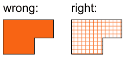
Large copper areas in grid form
Large copper areas on your circuit board should always be a grid if possible. This can usually be set in the layout program. For instance, a gridded area is called “hatch” by the Eagle program.
Of course, this is possible only if there are no sensitive high frequency conductor traces present.
The “grid” helps a great deal to avoid “Twist” and “Bow” effects, especially for circuit boards with only one layer.
Here you can find the Instructions on rasterized copper areas in EAGLE.
Fill copper-free areas with (grid) copper
Copper-free areas should be filled with (grid) copper.
Your advantages:
- A better homogeneity of the walls of the plated-through holes is achieved.
- Prevents twist & bow of the circuit board.
Design example of copper areas
| OK | Better | Perfect |
|---|
| OK | 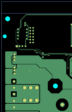 | Better | 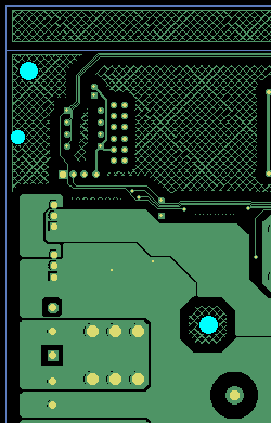 | Perfect | 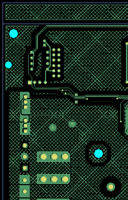 |
|---|
| OK | Without fill/grid | Better | Filled areas | Perfect | Filled areas + grid |
|---|
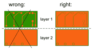
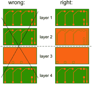
Ensure copper symmetry
Large copper areas should be counterbalanced with “copper filling” in the opposite layer.
Also try to distribute your conductor traces as uniformly as possible across the board.
For multilayer circuit boards, match the symmetrically opposite layer with “copper filling”.
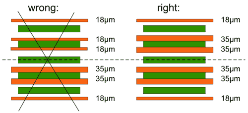
Symmetric copper distribution in layer buildups
The thicknesses of the copper foil in the layer buildup of your circuit board should always be symmetrically distributed. An asymmetric layer buildup can be manufactured, but we advise strongly against this because of possible deformations.