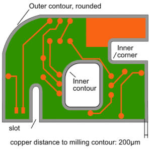
Outer corners of contours may be 90°, or rounded to your specifications.
The inner corners of contours have at least the radius of the milling tool.
Printed circuit board breakouts and contours are normally milled. Please observe the following rules:
| Parameter | Value | ||
|---|---|---|---|
| Parameter | Minimum milling tool diameter | Value | 0.8mm |
| Parameter | Smallest radius for inner corners | Value | 0.4mm |
| Parameter | Minimum spacing copper / milling contour | Value | 200µm |
| Application | Milling tool diameter Ø | Multi-CB Service | |||
|---|---|---|---|---|---|
| Application | Standard | Milling tool diameter Ø | ≥ 2.0mm | Multi-CB Service | Inclusive |
| Application | Special | Milling tool diameter Ø | ≥ 0.8mm < 2.0mm | Multi-CB Service | Inclusive |
Outer corners of contours may be 90°, or rounded to your specifications.
The inner corners of contours have at least the radius of the milling tool.
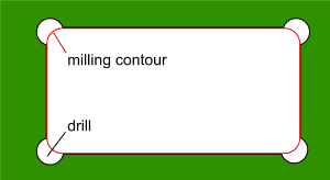
To hold exactly rectangular parts, the corresponding milled-out portion should also be drilled at the corners; this permits (for example) a precise framing for seven-segment display units.
| Option | Parameter | ||
|---|---|---|---|
| Option | min. width: | Parameter | 0,8mm |
| Option | Layer: | Parameter | Dimension layer, e.g. EAGLE layer 20 |
| Option | Copper claerance: | Parameter | 150µm |
| Option | Note: | Parameter | Copper exemption needs to be carried out. |
| Option | Parameter | ||
|---|---|---|---|
| Option | min. width: | Parameter | 0,8mm |
| Option | min. annular ring | Parameter | 200µm |
| Option | Layer: | Parameter | milling (mechanical layer), e.g. EAGLE layer 46 |
| Option | Note: | Parameter | Needs copper connections on TOP and BOT for through-plating. |
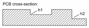
A variable level elevation can be milled at the edge or within a circuit board. This is called Z-axis milling.
To do this, create a new layer in your PCB design software for Z-axis milling only. Set the contour (1mil) for the milling area and also write down the desired milling depth (tolerance ±0.20mm).
Now activate the option "Z-axis milling" in the PCB calculator.
If the outer edge of the milling lies on the scoring line, the milling tool moves along the scored base material. This increases the risk of forming of chips.
Advice: Do not mill directly aligned with scribe lines.
We manufacture PCBs with milling and scoring on the same line. Should this result in shaving (chip) formation, a reclamation in this regard would be rejected.
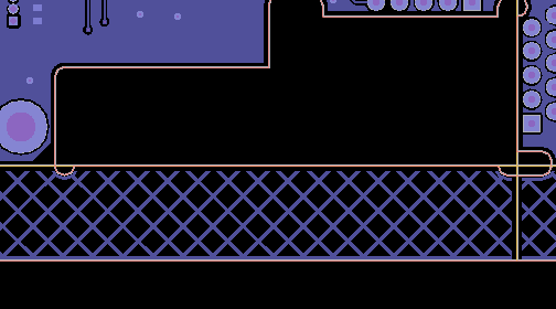
Milling meets scoring line at the panel frame (grid)
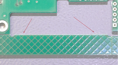
Milling and scoring on one line leads to chip formation


Some features of this website need your consent to remember who you are.

