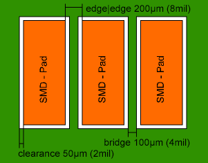
Solder-stop mask

We can only give a limited recommendation for coating vias  (plated-through holes) with solder-stop. Please refer to our Design Aid Via Covering.

You should pay special attention to solder-stop bridges (solder-stop between two pads or vias), which should not be smaller than 100µm (green solder-stop) and 150µm (coloured solder-stop) respectively.
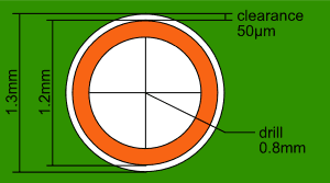
Solder-stop parameters (colour: green)

  clearance min clearance recommended bridge width min. bridge width recommended
Via 50µm - 100µm 125µm
Component hole 50µm 75µm 100µm 125µm
SMD pad 50µm 75µm 100µm 125µm

Solder-stop parameters (colour: red, blue, white, black)

  clearance min. clearance recommended bridge width min. bridge width recommended
Via 75µm - 150µm 150µm
Component hole 75µm 75µm 150µm 150µm
SMD Pad 75µm 75µm 150µm 150µm

Exemption of component holes

Exemption of component holes

For component holes, please ensure a clearance (spacing between copper to solder-stop) of at least 50µm (green solder-stop).

This clearance should be larger if possible (75µm), to avoid manufacture with extreme tolerances.

For other colours, the minimum solder-stop clearance is 75µm.

The smallest possible solder-stop bridge width is 100µm (green) or 150µm (other colours), respectively.


Exemption of SMD pads (fine pitch)

Exemption of SMD pads

The minimum solder-stop clearance for SMD pads should at least be 50µm, better: 75µm.

For other colours than green, the min. solder-stop clearance is 75µm.

The smallest possible solder-stop bridge width is 100µm (green) or 150µm (other colours), respectively.


BGA (Ball Grid Array)

Ball Grid Array

The following possibilities exist for BGAs (for explanation see Via Covering):

  • Via Tenting
  • Via Filling
  • Via-in-Pad


You should consult your assembly partner when selecting an appropriate surface, normally our customers select immersion tin or immersion gold.


Compare offers and order
SMD Stencils


Pricing Examples

Printed Circuit Boards always include:

- E-Test
- Solder-stop 2x
- Marking print 1x
- Gerber-Import
- Scoring (series)
- Design-Rule-Check

- Tooling costs
- Photoplot
- Conductors 150μm
- Drill holes 0,3mm
- Unlimited drilling
- HAL, FR4 1,6, 35μm Cu

Prototypes
2 layers - 6 WD
41,- €
1 Printed circuit board 100x100mm
4 layers - 8 WD
118,- €
1 Printed circuit board 160x100mm
6 layers - 8 WD
148,- €
1 Printed circuit board 160x100mm
Series
e.g. 100 pcs. Eurocard 100x160mm
2 layers - each
4,92 €
 
4 layers - each
7,05 €
 
6 layers - each
10,67 €
 
8 layers - each
16,99 €
 
SMD Stencils
max. 200x300mm - 3WD
47,50 €
1 Stencil, including 1000 pads
max. 600x600mm - 3WD
90,44 €
1 Stencil, including 2500 pads

Directly from your data

odbsprint-layoutgerberaltiumtargetcadsoft

Our free and comprehensive Design-Rule-Check helps avoiding many errors before the production even starts!
Click here for additional Design-Aid!

Directly from your data

Leiterplatten per UPSodbsprint-layoutgerberaltiumtargetcadsoft