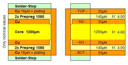
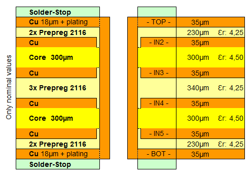
Layer buildups for PCB prototypes
In the following you can see the defined layer buildups for PCB prototypes with 4, 6 and 8 layers. These can be selected free of charge in our PCB calculator. If you wish to have different layer structures for your prototype, a large selection of prepregs, cores and foils are available in our special production.
Defined layer buildup
4 layers: 4L-01 (1.6mm)
6 layers: 6L-01 (1.6mm)
8 layers: 8L-01 (1.7mm)
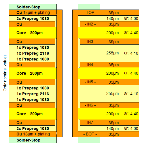
* Prepreg thicknesses after pressing, at approx. 80% copper utilization on the inner layers.


