Multiplier panel
Identical PCBs within panel
For cost-saving or technical reasons (such as improved assembly),multiple circuit boards may be combined to form a “panel”. This panel is then produced just as a single large circuit board. A separation of the panel does not occur!
Always clarify the panel design with your assembly partner; pay attention to fiducials marks or mounting holes!
Use our panel configurator during online order: With just a few inputs, you can configure your multiplier panel. In addition, a full-scale preview of your pcb panel is displayed within the order process. No additional panel -drawing / -release is necessary.
Panel types:

Multiplier panel
Identical PCBs within panel

Mixed multiplier panel
Different PCBs within panel
Mechanical processing
Already included: panel creation
X-out
The Multi-CB technology hotline will assist you: +49 (0) 8104 628 210
| Scored | Milled with bridges | Milled with bridges & mousebites | |||
|---|---|---|---|---|---|
| Scored | 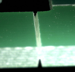 | Milled with bridges | 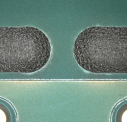 | Milled with bridges & mousebites | 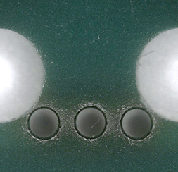 |
| Scored | - | Milled with bridges | Bridges are placed by Multi-CB | Milled with bridges & mousebites | Bridges and mousebites are placed by Multi-CB |
| Min. spacing of conductor / Cu to contour | Min. Spacing between PCBs | Line thickness of PCB contour | Recommended surounding frame | ||||||
|---|---|---|---|---|---|---|---|---|---|
| Scored panel | Min. spacing of conductor / Cu to contour | 500µm (0,5mm) | Min. Spacing between PCBs | 0,0mm / ≥ 5,5mm | Line thickness of PCB contour | 1 mil (0.01mm) | Recommended surounding frame | 5-10mm | |
| Milled panel | Min. spacing of conductor / Cu to contour | 200µm (0,2mm) | Min. Spacing between PCBs | 2,0mm | Line thickness of PCB contour | - | Recommended surounding frame | 5-10mm |
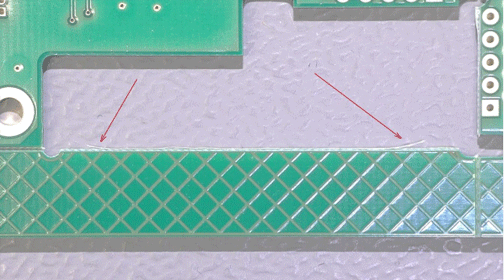
Multiple identical circuit board layouts are composed to form one panel. The completed panel is scored, or partially milled-out to provided the contained PCBs with bridges for breaking out.

When designing the panel, please observe that a spacing of 0,0mm is left between the circuit boards. If a spacing between the (scored) PCBs is required, please leave a gap of min. 5,0mm.
The contour line thickness should be 0,01mm / 1 mil.
Because of the tolerances when breaking out the single circuit boards, all conductor traces and copper areas should have a spacing of at least 500µm from the scoring edge (see scoring).
We recommend using scoring technology only for panels with a circuit board thickness of at least 1mm (stability).

When designing the panel, please observe that a spacing of 2,0mm is left between the circuit boards.
All conductor traces and copper areas should have a spacing of at least 200µm from the milling edge.
If no bridges are defined by the customer, these will be inserted by Multi CB! Optimum width for the bridges: 1,0 - 1,5mm.

When designing the panel, please observe that a spacing of 0,0mm is left between the circuit boards. If a spacing between the (scored) PCBs is required, please leave a gap of min. 5,0mm. For jump scoring a distance of 15mm is required.
The contour line thickness should be 0.01mm / 1 mil.
Because of the tolerances when breaking out the individual circuit boards, all conductor traces and copper areas should have a spacing of at least 500µm from the scoring edge (see scoring).
We recommend using scoring technology only for panels with a circuit board thickness of at least 1,0mm (stability).

When designing the panel, please observe that a spacing of 2,0mm is left between the circuit boards. For reasons of stability, a distance of 10mm is usually recommended.
All conductor traces and copper areas should have a spacing of at least 200µm from the milling edge.
If no bridges are defined by the customer, these will be inserted by Multi CB Optimum width for the bridges: 1,0 to 1,5mm.

When designing the panel, please observe that a spacing of 0,0mm is calculated between scored parts, and preferably 2,0mm between milled parts.
All conductor traces and copper areas should have a spacing of at least 500µm from the scoring edge, and at least 200µm from the milling edge!
If the outer edge of the milling lies on the scoring line, the milling tool moves along the scored base material. This increases the risk of forming of chips.
Advice: Do not mill directly aligned with scribe lines.
We manufacture PCBs with milling and scoring on the same line. Should this result in shaving (chip) formation, a reclamation in this regard would be rejected.
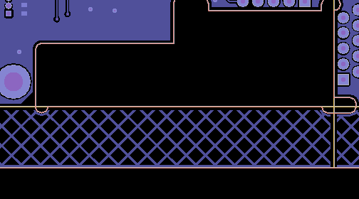
Milling meets scoring line at the panel frame (grid)
Milling and scoring on one line leads to chip formation


Some features of this website need your consent to remember who you are.

