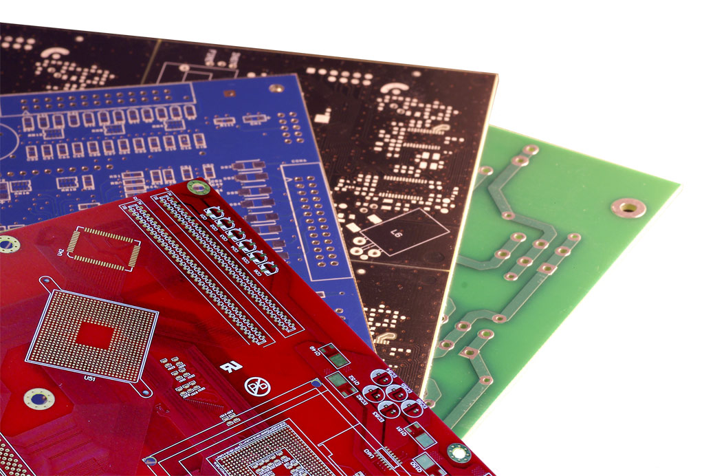
The following special circuit board types are available from Multi-CB:
Technical options for flexible circuit boards
Flexible circuit boards
| | Options | Inclusive | Notes |
|---|
| | Design | Options | 1 to 10 layers, plated-through | Inclusive | - | Notes | Layer buildup |
|---|
| | Conductor width min. | Options | 100µm | Inclusive | 100µm | Notes | |
|---|
| | Annular ring min. | Options | 100µm | Inclusive | 100µm | Notes | |
|---|
| | Via min. Ø | Options | 0.15mm | Inclusive | 0.2mm | Notes | |
|---|
| | Surfaces | Options | Chemical gold (recommended),
ENEPIG, chem silver | Inclusive | Chemical gold | Notes | Surfaces |
|---|
| | Materials | Options | Polyimide, high Tg polyimide | Inclusive | Polyimide | Notes | Materials |
|---|
| | Material thickness | Options | starting at 25µm foil plus copper | Inclusive | 25µm, 50µm | Notes | |
|---|
| | Copper thickness | Options | from 18µm | Inclusive | 18µm, 35µm | Notes | |
|---|
| | Stiffener | Options | 0.025µm - 3.20mm | Inclusive | 0.2mm, 0.3mm | Notes | |
|---|
| | Max. size | Options | 250mm x 450mm | Inclusive | - | Notes | larger on request |
|---|
| | Cover | Options | Coverlay or flexible solder-stop | Inclusive | - | Notes | |
|---|
| | Cover bridge min. | Options | Coverlay: ≥ 350µm
Flex. solder-stop: ≥ 100µm | Inclusive | - | Notes | Design-Aid |
|---|
| | Impedance control | Options | Yes (10% tolerance) | Inclusive | - | Notes | |
|---|
| | Adhesive tape | Options | 3M 9077 | Inclusive | - | Notes | Materials |
|---|
Technical options for Rigid-Flex circuit boards
Rigid-Flex circuit boards
| | Options | Notes |
|---|
| | Layers | Options | 2 to 24 layers, incl. "flying tails" | Notes | Layer buildup |
|---|
| | Conductor width min. | Options | 75µm | Notes | |
|---|
| | Annular ring min. | Options | 125µm | Notes | |
|---|
| | Via min. Ø | Options | 0.1mm | Notes | |
|---|
| | Surfaces | Options | Chemical gold (recommended), immersion tin, HAL lead-free | Notes | Surfaces |
|---|
| | Materials | Options | Polyimide, high Tg polyimide, FR4, FR4 high Tg | Notes | Materials |
|---|
| | Material thickness | Options | Polyimide starting at 62µm doublesided, FR4 starting at 100µm | Notes | |
|---|
| | Max. size | Options | 250mm x 450mm | Notes | larger on request |
|---|
| | Solder-stop | Options | Coverlay or flexible solder-stop | Notes | |
|---|
Technical options for metal core circuit boards
Metal core circuit boards
| | Options | Inklusive | Notes |
|---|
| | Material | Options | Aluminium core | Inklusive | - | Notes | Data sheets |
|---|
| | Max. size | Options | 420mm x 570mm | Inklusive | - | Notes | |
|---|
| | Design | Options | 1 layer, 2 layers plated-through | Inklusive | | Notes | |
|---|
| | Aluminium thickness | Options | 0.5mm, 0.8mm, 1.0mm, 1.5mm, 2.0mm | Inklusive | 1.5mm | Notes | |
|---|
| | Copper | Options | 35µm, 70µm, 105µm, 140µm | Inklusive | 35µm | Notes | |
|---|
| | Insulation thickness | Options | 75µm, 100µm, 125µm, 150µm | Inklusive | 100µm | Notes | |
|---|
| | Thermal conductivity | Options | 2.0W/mK - 7.0W/mK | Inklusive | 2.0W/mK | Notes | |
|---|
| | Conductor width min. | Options | 150µm | Inklusive | 150µm | Notes | |
|---|
| | Annular ring min. | Options | 125µm | Inklusive | 150µm | Notes | |
|---|
| | Drill (NPTH) min. Ø | Options | 0.5mm | Inklusive | 0.9mm | Notes | Design-Aid |
|---|
| | Via min. Ø | Options | 0.2mm | Inklusive | 0.2mm | Notes | |
|---|
| | Surface | Options | HAL lead-free, chemical gold | Inklusive | HAL lead-free | Notes | Surfaces |
|---|
| | Solder-stop | Options | white, black, green, red, blue | Inklusive | white, black | Notes | |
|---|
| | Legend print | Options | black, white | Inklusive | - | Notes | |
|---|
| | Milling | Options | yes | Inklusive | yes | Notes | |
|---|
| | V-Scoring | Options | yes | Inklusive | yes | Notes | clean & simple |
|---|
| | Z-Axis milling | Options | yes | Inklusive | - | Notes | |
|---|
| | RoHS compliant | Options | yes | Inklusive | yes | Notes | |
|---|
| | UL-certified | Options | yes | Inklusive | yes | Notes | UL certificate |
|---|
| Material for metal core boards
1 Layer |  Thermal conductivity Thermal conductivity |  Thermal resistance Thermal resistance |  Surface resistivity Surface resistivity |  Dielectric glass transition Dielectric glass transition |  Dielectric Breakdown (AC)* Dielectric Breakdown (AC)* |  CTI CTI |
|---|
| Material for metal core boards
1 Layer | | Thermal conductivity | W/mK | Thermal resistance | K/W | Surface resistivity | MΩ | Dielectric glass transition | °C | Dielectric Breakdown (AC)* | kV | CTI | PLC |
|---|
| Material for metal core boards
1 Layer | TC-Lam 2.0 | Thermal conductivity | 2.0 | Thermal resistance | 0.50 | Surface resistivity | 10^7 | Dielectric glass transition | 100 | Dielectric Breakdown (AC)* | 5.0 | CTI | 0 |
|---|
| Material for metal core boards
1 Layer | HA50 (3) | Thermal conductivity | 2.2 | Thermal resistance | 0.41 | Surface resistivity | 10^6 | Dielectric glass transition | 120 | Dielectric Breakdown (AC)* | 4.3 | CTI | 0 |
|---|
| Material for metal core boards
1 Layer | AL-200 | Thermal conductivity | 2.0 | Thermal resistance | 0.35 | Surface resistivity | 10^8 | Dielectric glass transition | - | Dielectric Breakdown (AC)* | 3.5 | CTI | 0 |
|---|
| Material for metal core boards
1 Layer | AL-300 | Thermal conductivity | 3.0 | Thermal resistance | 0.30 | Surface resistivity | 10^8 | Dielectric glass transition | - | Dielectric Breakdown (AC)* | 3.5 | CTI | 0 |
|---|
| Material for metal core boards
1 Layer | Ventec VT-4B3
Ceramic Filled | Thermal conductivity | 3.0 | Thermal resistance | - | Surface resistivity | 5 x 10^8 | Dielectric glass transition | 130 | Dielectric Breakdown (AC)* | 8.0 | CTI | 0 |
|---|
| Material for metal core boards
1 Layer | Ventec VT-4B4
Ceramic Filled | Thermal conductivity | 4.2 | Thermal resistance | - | Surface resistivity | 2 x 10^7 | Dielectric glass transition | 120 | Dielectric Breakdown (AC)* | 8.0 | CTI | 0 |
|---|
| Material for metal core boards
1 Layer | Ventec VT-4B7
Ceramic Filled | Thermal conductivity | 7.0 | Thermal resistance | - | Surface resistivity | 2 x 10^7 | Dielectric glass transition | 100 | Dielectric Breakdown (AC)* | 8.0 | CTI | 0 |
|---|
* Examples for 100μm dielectric or 80μm for CCAF material
| Material for metal core boards
2 Layers (plated-through) | Thermal conductivity | Thermal resistance | Surface resistivity | Dielectric glass transition | Dielectric Breakdown (AC)* | CTI |
|---|
| Material for metal core boards
2 Layers (plated-through) | | Thermal conductivity | W/mK | Thermal resistance | K/W | Surface resistivity | MΩ | Dielectric glass transition | °C | Dielectric Breakdown (AC)* | kV | CTI | PLC |
|---|
| Material for metal core boards
2 Layers (plated-through) | Ventec VT-4A2 | Thermal conductivity | 2.2 | Thermal resistance | - | Surface resistivity | 2 x 10^7 | Dielectric glass transition | 130 | Dielectric Breakdown (AC)* | 7.5 | CTI | 0 |
|---|
| Material for metal core boards
2 Layers (plated-through) | Ventec VT-4B3
Ceramic Filled | Thermal conductivity | 3.0 | Thermal resistance | - | Surface resistivity | 5 x 10^8 | Dielectric glass transition | 130 | Dielectric Breakdown (AC)* | 8.0 | CTI | 0 |
|---|
* Examples for 100μm dielectric or 80μm for CCAF material
Technical options for High Freqency circuit boards
High Freqency circuit boards
| Material for high frequency boards |  Order share Order share |  ?r ?r |  Dk Loss Tangent Dk Loss Tangent |  Tg Tg |  Td value Td value | Thermal conductivity |  CTE-z CTE-z |  Electric strenght Electric strenght | Surface resistivity |  Peel strength Peel strength |
|---|
| Material for high frequency boards | | Order share | | ?r | @10GHz | Dk Loss Tangent | @10GHz | Tg | °C | Td value | °C | Thermal conductivity | W/m*K | CTE-z | ppm/°C | Electric strenght | kV/mm | Surface resistivity | MO | Peel strength | N/mm |
|---|
| Material for high frequency boards | Rogers 4350B
HF material | Order share | +++ | ?r | 3,5 | Dk Loss Tangent | 0,0037 | Tg | 280° | Td value | 390° | Thermal conductivity | 0,69 | CTE-z | 32 | Electric strenght | 31 | Surface resistivity | 5,7 x 10^9 | Peel strength | 0,9 |
|---|
| Material for high frequency boards | Rogers 4003C
HF material | Order share | ++ | ?r | 3,4 | Dk Loss Tangent | 0,0027 | Tg | 280° | Td value | 425° | Thermal conductivity | 0,71 | CTE-z | 46 | Electric strenght | 31 | Surface resistivity | 4,2 x 10^9 | Peel strength | 1,1 |
|---|
| Material for high frequency boards | Panasonic Megtron6
HF material | Order share | + | ?r | 3,6 | Dk Loss Tangent | 0,004 | Tg | 185° | Td value | 410° | Thermal conductivity | - | CTE-z | 45 | Electric strenght | - | Surface resistivity | 1 x 10^8 | Peel strength | 0,8 |
|---|
| Material for high frequency boards | Rogers RO3003
PTFE ceramic-filled | Order share | + | ?r | 3 | Dk Loss Tangent | 0,0013 | Tg | - | Td value | 500° | Thermal conductivity | 0,5 | CTE-z | 25 | Electric strenght | - | Surface resistivity | 1 x 10^7 | Peel strength | 2,2 |
|---|
| Material for high frequency boards | Rogers RO3006
PTFE ceramic-filled | Order share | o | ?r | 6,2 | Dk Loss Tangent | 0,002 | Tg | - | Td value | 500° | Thermal conductivity | 0,79 | CTE-z | 24 | Electric strenght | - | Surface resistivity | 1 x 10^5 | Peel strength | 1,2 |
|---|
| Material for high frequency boards | Rogers RO3010
PTFE ceramic-filled | Order share | o | ?r | 10 | Dk Loss Tangent | 0,0022 | Tg | - | Td value | 500° | Thermal conductivity | 0,95 | CTE-z | 16 | Electric strenght | - | Surface resistivity | 1 x 10^5 | Peel strength | 1,6 |
|---|
| Material for high frequency boards | Taconic RF-35
Ceramic | Order share | o | ?r | 3,5* | Dk Loss Tangent | 0,0018* | Tg | 315° | Td value | - | Thermal conductivity | 0,24 | CTE-z | 64 | Electric strenght | - | Surface resistivity | 1,5 x 10^8 | Peel strength | 1,8 |
|---|
| Material for high frequency boards | Taconic TLX
PTFE | Order share | o | ?r | 2,5 | Dk Loss Tangent | 0,0019 | Tg | - | Td value | - | Thermal conductivity | 0,19 | CTE-z | 135 | Electric strenght | - | Surface resistivity | 1 x 10^7 | Peel strength | 2,1 |
|---|
| Material for high frequency boards | Rogers RO3001
Bonding Film for PTFE | Order share | - | ?r | 2,3 | Dk Loss Tangent | 0,003 | Tg | 160° | Td value | - | Thermal conductivity | 0,22 | CTE-z | - | Electric strenght | 98 | Surface resistivity | 1 x 10^9 | Peel strength | 2,1 |
|---|
| Material for high frequency boards | Taconic TLC
PTFE | Order share | - | ?r | 3,2 | Dk Loss Tangent | - | Tg | - | Td value | - | Thermal conductivity | 0,24 | CTE-z | 70 | Electric strenght | - | Surface resistivity | 1 x 10^7 | Peel strength | 2,1 |
|---|
Technical options for High-Tg circuit boards
High-Tg circuit boards
| Material for High-Tg boards | Tg | CTE-z | ?r | Electric strenght | Surface resistivity | CTI | Thermal conductivity | Td value | Peel strength |
|---|
| Material for High-Tg boards | | Tg | °C | CTE-z | ppm/°C | ?r | @1GHz | Electric strenght | KV/mm | Surface resistivity | MO | CTI | PLC | Thermal conductivity | W/m*K | Td value | °C | Peel strength | N/mm |
|---|
| Material for High-Tg boards | ISOLA IS410
FR4 HTg, CAF-Enhanced | Tg | 180° | CTE-z | 55 | ?r | 4,0 | Electric strenght | 44 | Surface resistivity | 8,0 x 10^6 | CTI | 3 | Thermal conductivity | 0,5 | Td value | 350° | Peel strength | 1,2 |
|---|
| Material for High-Tg boards | ISOLA IS420
FR4 HTg, CAF-Enhanced | Tg | 170° | CTE-z | 45 | ?r | 4,0 | Electric strenght | 54 | Surface resistivity | 3,0 x 10^6 | CTI | 3 | Thermal conductivity | 0,4 | Td value | 350° | Peel strength | 1,3 |
|---|
| Material for High-Tg boards | ITEQ IT-180A
FR4 HTg | Tg | 175° | CTE-z | 45 | ?r | 4,4 | Electric strenght | 45 | Surface resistivity | 3,0 x 10^10 | CTI | - | Thermal conductivity | - | Td value | 345° | Peel strength | 1,4 |
|---|
| Material for High-Tg boards | Shengyi S1000-2
FR4 HTg | Tg | 180° | CTE-z | 45 | ?r | 4,8* | Electric strenght | 63 | Surface resistivity | 7,9 x 10^7 | CTI | 3 | Thermal conductivity | - | Td value | 345° | Peel strength | 1,4 |
|---|
| Material for High-Tg boards | ARLON 85N
Polyimid HTg | Tg | 250° | CTE-z | 55 | ?r | 4,20* | Electric strenght | 57 | Surface resistivity | 1,6 x 10^9 | CTI | - | Thermal conductivity | 0,2 | Td value | 387° | Peel strength | 1,2 |
|---|
CAF - Conductive Anodic Filament: an undesirable conducting filament in the substrate of a circuit board
Technical options for thick copper circuit boards
Thick copper circuit boards
| Final thickness* | Min. conductor width | Min. conductor spacing |
|---|
| Final thickness* | 105µm | Min. conductor width | 250µm | Min. conductor spacing | 250µm |
|---|
| Final thickness* | 140µm | Min. conductor width | 350µm | Min. conductor spacing | 350µm |
|---|
| Final thickness* | 210µm | Min. conductor width | 500µm | Min. conductor spacing | 500µm |
|---|
| Final thickness* | 400µm** | Min. conductor width | 900µm | Min. conductor spacing | 900µm |
|---|
| Copper foil thickness | Min. conductor width | Min. conductor spacing |
|---|
| Copper foil thickness | 105µm | Min. conductor width | 250µm | Min. conductor spacing | 250µm |
|---|
| Copper foil thickness | 140µm | Min. conductor width | 300µm | Min. conductor spacing | 300µm |
|---|
| Copper foil thickness | 210µm | Min. conductor width | 500µm | Min. conductor spacing | 500µm |
|---|
| Copper foil thickness | 400µm** | Min. conductor width | 900µm | Min. conductor spacing | 900µm |
|---|
* after electroplating
** only on request
Folgende speziellen Leiterplatten-Typen sind bei Multi-CB verfügbar:
Technische Optionen - Flexible-Leiterplatten
Flexible Leiterplatten
| | Option | Inklusive | Hinweise |
|---|
| | Ausführung | Option | 1-10 Lagen durchkontaktiert | Inklusive | - | Hinweise | Lagenaufbau |
|---|
| | Leiterbahn min. | Option | 100µm | Inklusive | 100µm | Hinweise | |
|---|
| | Restring min. | Option | 100µm | Inklusive | 100µm | Hinweise | |
|---|
| | Via min. Ø | Option | 0.15mm | Inklusive | 0.2mm | Hinweise | |
|---|
| | Oberflächen | Option | chemisch Gold (empfohlen),
ENEPIG, chem. Silber | Inklusive | chemisch Gold | Hinweise | Oberflächen |
|---|
| | Materialien | Option | Polyimid, Polyimid Hoch-TG | Inklusive | Polyimid | Hinweise | Materialien |
|---|
| | Materialdicke | Option | ab 25µm Folie zzgl. Kupfer | Inklusive | 25µm, 50µm | Hinweise | |
|---|
| | Kupferdicke | Option | ab 18µm | Inklusive | 18µm, 35µm | Hinweise | |
|---|
| | Stiffener | Option | 0.025mm - 3.2mm | Inklusive | 0.2mm, 0.3mm | Hinweise | |
|---|
| | Max. Größe | Option | 250mm x 450mm | Inklusive | - | Hinweise | größer a.A. |
|---|
| | Abdeckung | Option | PI Coverlay (z.B. mehrere Biegezyklen) oder
flexibler Lötstopp (z.B. stabile Biegung) | Inklusive | PI coverlay 25µm | Hinweise | |
|---|
| | Stegbreite min. | Option | Coverlay: ≥ 350µm
flexibler Lötstopp: ≥ 100µm | Inklusive | - | Hinweise | Design-Hilfe |
|---|
| | Impedanzkontrolle | Option | ja (10% Toleranz) | Inklusive | - | Hinweise | |
|---|
| | Klebetape | Option | 3M 9077 | Inklusive | - | Hinweise | Materialien |
|---|
Technische Optionen - Starrflex-Leiterplatten
Starrflex-Leiterplatten
| | Option | Hinweise |
|---|
| | Ausführung | Option | 2-24 Lagen Multilayer, auch "Flying tails" | Hinweise | Lagenaufbau |
|---|
| | Leiterbahn min. | Option | 75µm | Hinweise | |
|---|
| | Restring min. | Option | 125µm | Hinweise | |
|---|
| | Via min. Ø | Option | 0.1mm | Hinweise | |
|---|
| | Oberflächen | Option | chemisch Gold (empfohlen), chem. Zinn, HAL bleifrei | Hinweise | Oberflächen |
|---|
| | Materialien | Option | Polyimid, Polyimid Hoch-TG, FR4, FR4 Hoch-TG | Hinweise | Materialien |
|---|
| | Materialdicke | Option | Polyimid ab 62µm doppelseitig, FR4 ab 100µm | Hinweise | |
|---|
| | Max. Größe | Option | 250mm x 450mm | Hinweise | größer a.A. |
|---|
| | Abdeckung | Option | Coverlay oder flexibler Lötstopp | Hinweise | |
|---|
Technische Optionen - Metallkern-Leiterplatten
Metallkern-Leiterplatten
| | Option | Inklusive | Hinweise |
|---|
| | Material | Option | Aluminium Kern | Inklusive | - | Hinweise | Datenblätter |
|---|
| | Max. Größe | Option | 420mm x 570mm | Inklusive | - | Hinweise | |
|---|
| | Ausführung | Option | 1Lage, 2 Lagen durchkontaktiert | Inklusive | - | Hinweise | |
|---|
| | Aluminium Dicke | Option | 0.5mm, 0.8mm, 1.0mm, 1.5mm, 2.0mm | Inklusive | 1.5mm | Hinweise | |
|---|
| | Kupferdicke | Option | 35µm, 70µm, 105µm, 140µm | Inklusive | 35µm | Hinweise | |
|---|
| | Isolationsdicke | Option | 75µm, 100µm, 125µm, 150µm | Inklusive | 100µm | Hinweise | |
|---|
| | Wärmeleitwert | Option | 2.0W/mK - 7.0W/mK | Inklusive | 2.0W/mK | Hinweise | |
|---|
| | Leiterbahn min. | Option | 150µm | Inklusive | 150µm | Hinweise | |
|---|
| | Restring min. | Option | 125µm | Inklusive | 150µm | Hinweise | |
|---|
| | Bohrung (NDK) min. Ø | Option | 0.5mm | Inklusive | 0.9mm | Hinweise | Design-Hilfe |
|---|
| | Via min. Ø | Option | 0.2mm | Inklusive | 0.3mm | Hinweise | |
|---|
| | Oberfläche | Option | HAL bleifrei, chem. Gold | Inklusive | HAL bleifrei | Hinweise | Oberflächen |
|---|
| | Lötstopp | Option | weiß, schwarz, grün, rot, blau | Inklusive | weiß, schwarz | Hinweise | |
|---|
| | Positionsdruck | Option | schwarz, weiß | Inklusive | - | Hinweise | |
|---|
| | Fräsen | Option | ja | Inklusive | ja | Hinweise | |
|---|
| | Ritzen | Option | ja | Inklusive | ja | Hinweise | einfach & sauber |
|---|
| | Z-Achsen Fräsen | Option | ja | Inklusive | - | Hinweise | |
|---|
| | RoHS-Konform | Option | ja | Inklusive | ja | Hinweise | |
|---|
| | UL-Zertifiziert | Option | ja | Inklusive | ja | Hinweise | UL Zertifikat |
|---|
| Material for metal core boards
1 Layer | Thermal conductivity | Thermal resistance | Surface resistivity | Dielectric glass transition | Dielectric Breakdown (AC)* | CTI |
|---|
| Material for metal core boards
1 Layer | | Thermal conductivity | W/mK | Thermal resistance | K/W | Surface resistivity | MΩ | Dielectric glass transition | °C | Dielectric Breakdown (AC)* | kV | CTI | PLC |
|---|
| Material for metal core boards
1 Layer | TC-Lam 2.0 | Thermal conductivity | 2.0 | Thermal resistance | 0.50 | Surface resistivity | 10^7 | Dielectric glass transition | 100 | Dielectric Breakdown (AC)* | 5.0 | CTI | 0 |
|---|
| Material for metal core boards
1 Layer | HA50 (3) | Thermal conductivity | 2.2 | Thermal resistance | 0.41 | Surface resistivity | 10^6 | Dielectric glass transition | 120 | Dielectric Breakdown (AC)* | 4.3 | CTI | 0 |
|---|
| Material for metal core boards
1 Layer | AL-200 | Thermal conductivity | 2.0 | Thermal resistance | 0.35 | Surface resistivity | 10^8 | Dielectric glass transition | - | Dielectric Breakdown (AC)* | 3.5 | CTI | 0 |
|---|
| Material for metal core boards
1 Layer | AL-300 | Thermal conductivity | 3.0 | Thermal resistance | 0.30 | Surface resistivity | 10^8 | Dielectric glass transition | - | Dielectric Breakdown (AC)* | 3.5 | CTI | 0 |
|---|
| Material for metal core boards
1 Layer | Ventec VT-4B3
Ceramic Filled | Thermal conductivity | 3.0 | Thermal resistance | - | Surface resistivity | 5 x 10^8 | Dielectric glass transition | 130 | Dielectric Breakdown (AC)* | 8.0 | CTI | 0 |
|---|
| Material for metal core boards
1 Layer | Ventec VT-4B4
Ceramic Filled | Thermal conductivity | 4.2 | Thermal resistance | - | Surface resistivity | 2 x 10^7 | Dielectric glass transition | 120 | Dielectric Breakdown (AC)* | 8.0 | CTI | 0 |
|---|
| Material for metal core boards
1 Layer | Ventec VT-4B7
Ceramic Filled | Thermal conductivity | 7.0 | Thermal resistance | - | Surface resistivity | 2 x 10^7 | Dielectric glass transition | 100 | Dielectric Breakdown (AC)* | 8.0 | CTI | 0 |
|---|
* Examples for 100μm dielectric or 80μm for CCAF material
| Material for metal core boards
2 Layers (plated-through) | Thermal conductivity | Thermal resistance | Surface resistivity | Dielectric glass transition | Dielectric Breakdown (AC)* | CTI |
|---|
| Material for metal core boards
2 Layers (plated-through) | | Thermal conductivity | W/mK | Thermal resistance | K/W | Surface resistivity | MΩ | Dielectric glass transition | °C | Dielectric Breakdown (AC)* | kV | CTI | PLC |
|---|
| Material for metal core boards
2 Layers (plated-through) | Ventec VT-4A2 | Thermal conductivity | 2.2 | Thermal resistance | - | Surface resistivity | 2 x 10^7 | Dielectric glass transition | 130 | Dielectric Breakdown (AC)* | 7.5 | CTI | 0 |
|---|
| Material for metal core boards
2 Layers (plated-through) | Ventec VT-4B3
Ceramic Filled | Thermal conductivity | 3.0 | Thermal resistance | - | Surface resistivity | 5 x 10^8 | Dielectric glass transition | 130 | Dielectric Breakdown (AC)* | 8.0 | CTI | 0 |
|---|
* Examples for 100μm dielectric or 80μm for CCAF material
Technische Optionen - Hochfrequenz-Leiterplatten
Hochfrequenz-Leiterplatten
| Material for high frequency boards | Order share | ?r | Dk Loss Tangent | Tg | Td value | Thermal conductivity | CTE-z | Electric strenght | Surface resistivity | Peel strength |
|---|
| Material for high frequency boards | | Order share | | ?r | @10GHz | Dk Loss Tangent | @10GHz | Tg | °C | Td value | °C | Thermal conductivity | W/m*K | CTE-z | ppm/°C | Electric strenght | kV/mm | Surface resistivity | MO | Peel strength | N/mm |
|---|
| Material for high frequency boards | Rogers 4350B
HF material | Order share | +++ | ?r | 3,5 | Dk Loss Tangent | 0,0037 | Tg | 280° | Td value | 390° | Thermal conductivity | 0,69 | CTE-z | 32 | Electric strenght | 31 | Surface resistivity | 5,7 x 10^9 | Peel strength | 0,9 |
|---|
| Material for high frequency boards | Rogers 4003C
HF material | Order share | ++ | ?r | 3,4 | Dk Loss Tangent | 0,0027 | Tg | 280° | Td value | 425° | Thermal conductivity | 0,71 | CTE-z | 46 | Electric strenght | 31 | Surface resistivity | 4,2 x 10^9 | Peel strength | 1,1 |
|---|
| Material for high frequency boards | Panasonic Megtron6
HF material | Order share | + | ?r | 3,6 | Dk Loss Tangent | 0,004 | Tg | 185° | Td value | 410° | Thermal conductivity | - | CTE-z | 45 | Electric strenght | - | Surface resistivity | 1 x 10^8 | Peel strength | 0,8 |
|---|
| Material for high frequency boards | Rogers RO3003
PTFE ceramic-filled | Order share | + | ?r | 3 | Dk Loss Tangent | 0,0013 | Tg | - | Td value | 500° | Thermal conductivity | 0,5 | CTE-z | 25 | Electric strenght | - | Surface resistivity | 1 x 10^7 | Peel strength | 2,2 |
|---|
| Material for high frequency boards | Rogers RO3006
PTFE ceramic-filled | Order share | o | ?r | 6,2 | Dk Loss Tangent | 0,002 | Tg | - | Td value | 500° | Thermal conductivity | 0,79 | CTE-z | 24 | Electric strenght | - | Surface resistivity | 1 x 10^5 | Peel strength | 1,2 |
|---|
| Material for high frequency boards | Rogers RO3010
PTFE ceramic-filled | Order share | o | ?r | 10 | Dk Loss Tangent | 0,0022 | Tg | - | Td value | 500° | Thermal conductivity | 0,95 | CTE-z | 16 | Electric strenght | - | Surface resistivity | 1 x 10^5 | Peel strength | 1,6 |
|---|
| Material for high frequency boards | Taconic RF-35
Ceramic | Order share | o | ?r | 3,5* | Dk Loss Tangent | 0,0018* | Tg | 315° | Td value | - | Thermal conductivity | 0,24 | CTE-z | 64 | Electric strenght | - | Surface resistivity | 1,5 x 10^8 | Peel strength | 1,8 |
|---|
| Material for high frequency boards | Taconic TLX
PTFE | Order share | o | ?r | 2,5 | Dk Loss Tangent | 0,0019 | Tg | - | Td value | - | Thermal conductivity | 0,19 | CTE-z | 135 | Electric strenght | - | Surface resistivity | 1 x 10^7 | Peel strength | 2,1 |
|---|
| Material for high frequency boards | Rogers RO3001
Bonding Film for PTFE | Order share | - | ?r | 2,3 | Dk Loss Tangent | 0,003 | Tg | 160° | Td value | - | Thermal conductivity | 0,22 | CTE-z | - | Electric strenght | 98 | Surface resistivity | 1 x 10^9 | Peel strength | 2,1 |
|---|
| Material for high frequency boards | Taconic TLC
PTFE | Order share | - | ?r | 3,2 | Dk Loss Tangent | - | Tg | - | Td value | - | Thermal conductivity | 0,24 | CTE-z | 70 | Electric strenght | - | Surface resistivity | 1 x 10^7 | Peel strength | 2,1 |
|---|
Technische Optionen - Hoch-Tg-Leiterplatten
Hoch-TG-Leiterplatten
| Material for High-Tg boards | Tg | CTE-z | ?r | Electric strenght | Surface resistivity | CTI | Thermal conductivity | Td value | Peel strength |
|---|
| Material for High-Tg boards | | Tg | °C | CTE-z | ppm/°C | ?r | @1GHz | Electric strenght | KV/mm | Surface resistivity | MO | CTI | PLC | Thermal conductivity | W/m*K | Td value | °C | Peel strength | N/mm |
|---|
| Material for High-Tg boards | ISOLA IS410
FR4 HTg, CAF-Enhanced | Tg | 180° | CTE-z | 55 | ?r | 4,0 | Electric strenght | 44 | Surface resistivity | 8,0 x 10^6 | CTI | 3 | Thermal conductivity | 0,5 | Td value | 350° | Peel strength | 1,2 |
|---|
| Material for High-Tg boards | ISOLA IS420
FR4 HTg, CAF-Enhanced | Tg | 170° | CTE-z | 45 | ?r | 4,0 | Electric strenght | 54 | Surface resistivity | 3,0 x 10^6 | CTI | 3 | Thermal conductivity | 0,4 | Td value | 350° | Peel strength | 1,3 |
|---|
| Material for High-Tg boards | ITEQ IT-180A
FR4 HTg | Tg | 175° | CTE-z | 45 | ?r | 4,4 | Electric strenght | 45 | Surface resistivity | 3,0 x 10^10 | CTI | - | Thermal conductivity | - | Td value | 345° | Peel strength | 1,4 |
|---|
| Material for High-Tg boards | Shengyi S1000-2
FR4 HTg | Tg | 180° | CTE-z | 45 | ?r | 4,8* | Electric strenght | 63 | Surface resistivity | 7,9 x 10^7 | CTI | 3 | Thermal conductivity | - | Td value | 345° | Peel strength | 1,4 |
|---|
| Material for High-Tg boards | ARLON 85N
Polyimid HTg | Tg | 250° | CTE-z | 55 | ?r | 4,20* | Electric strenght | 57 | Surface resistivity | 1,6 x 10^9 | CTI | - | Thermal conductivity | 0,2 | Td value | 387° | Peel strength | 1,2 |
|---|
CAF - Conductive Anodic Filament: an undesirable conducting filament in the substrate of a circuit board
Technische Optionen - Dickkupfer-Leiterplatten
Dickkupfer-Leiterplatten
| End-Dicke* | Leiterbahnbreite min. | Leiterbahnabst. min. |
|---|
| End-Dicke* | 105µm | Leiterbahnbreite min. | 250µm | Leiterbahnabst. min. | 250µm |
|---|
| End-Dicke* | 140µm | Leiterbahnbreite min. | 350µm | Leiterbahnabst. min. | 350µm |
|---|
| End-Dicke* | 210µm | Leiterbahnbreite min. | 500µm | Leiterbahnabst. min. | 500µm |
|---|
| End-Dicke* | 400µm** | Leiterbahnbreite min. | 900µm | Leiterbahnabst. min. | 900µm |
|---|
| Kupferfolie-Dicke | Leiterbahnbreite min. | Leiterbahnabst. min. |
|---|
| Kupferfolie-Dicke | 105µm | Leiterbahnbreite min. | 250µm | Leiterbahnabst. min. | 250µm |
|---|
| Kupferfolie-Dicke | 140µm | Leiterbahnbreite min. | 300µm | Leiterbahnabst. min. | 300µm |
|---|
| Kupferfolie-Dicke | 210µm | Leiterbahnbreite min. | 500µm | Leiterbahnabst. min. | 500µm |
|---|
| Kupferfolie-Dicke | 400µm** | Leiterbahnbreite min. | 900µm | Leiterbahnabst. min. | 900µm |
|---|
* nach Galvanisierung
** nur auf Anfrage