If you create your circuit board layout with the Sprint Layout program from ABACOM, please observe the following tips. Basically, it makes sense to use all the prescribed standard-layers of sprint Layout.
We are happy to take care of generating the production data (Extended Gerber) for you. You just have to send us your *.lay file along with your order. All further steps are taken care of by our CAM engineers.
Sprint Layout
We naturally import your ODB++, Gerber-, KiCad-, OrCAD-, Target-, Eagle-, Altium-, IPC-2581-, DPF- and Sprint layout data free of charge!
Multi-CB parameters
For an optimal result, please define the free-of-charge high-tech parameters of Multi-CB:
- Track-width / space: 0,1mm (100µm) - free-of-charge ✓
- Annular ring: 0,1mm (100µm) - free-of-charge ✓
- Drills: 0.2mm (200µm) - free-of-charge ✓
- Via-Pad: 0,4mm (400µm) - free-of-charge ✓
This guarantees the best technology at the best price. The minimum possible values can be found here: Circuit board design parameters.
Standard layers
To convert your Sprint Layout files, we use the standard layers. Please specify any variations or extended layer specifications with your order.
| Layer type | Name | Layer | Notes | ||||
|---|---|---|---|---|---|---|---|
| Layer type | TOP | Name | Copper Top | Layer | C1 | Notes | |
| Layer type | BOT | Name | Copper Bot | Layer | C2 | Notes | |
| Layer type | Inner layer 1 | Name | Copper Inner 1 | Layer | I1 | Notes | |
| Layer type | Inner layer 2 | Name | Copper Inner 2 | Layer | I2 | Notes | |
| Layer type | Vias | Name | Drills | Layer | Drills | Notes | PTH |
| Layer type | Drills (non-plated-through) | Name | Holes | Layer | Holes | Notes | NPTH |
| Layer type | Contour & Milling | Name | Outline | Layer | O | Notes | line width 1mil (25µm) |
| Layer type | Scoring | Name | Layer | O | Notes | ||
| Layer type | Solder-stop TOP | Name | Solder mask | Layer | C1 Solder mask | Notes | |
| Layer type | Solder-stop BOT | Name | Solder mask | Layer | C2 Solder mask | Notes | |
| Layer type | Marking print TOP | Name | Silkscreen Top | Layer | S1 | Notes | |
| Layer type | Marking print BOT | Name | Silkscreen Bot | Layer | S2 | Notes | |
| Layer type | SMD Stencil TOP | Name | SMD mask | Layer | C1 SMD mask | Notes | |
| Layer type | SMD Stencil BOT | Name | SMD mask | Layer | C2 SMD mask | Notes |
Gerber Export
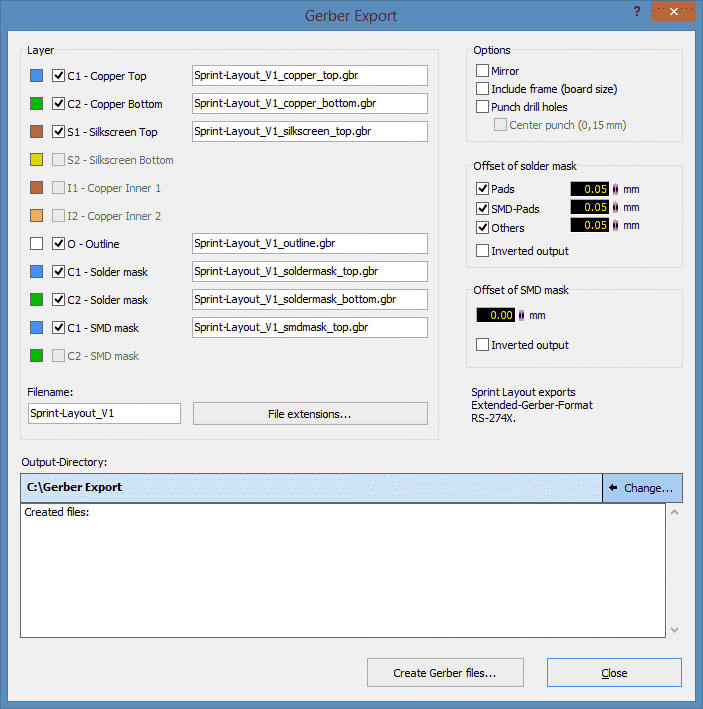
If you want to make the Gerber export by yourself, please use the default settings of Sprint-Layout. In the example image: 2 layer PCB.
Options
Please do not choose "mirror" in any case. See also layer orientation.
Offset of solder mask
Please set the offset (or clearance) of the solder mask to 0.05 mm (50µm), this is the minimum tolerance where no solder mask is applied to the solder pad. The value should not be (much) larger as well, so that fine-pitch components have still a solder mask bridge between the pads. If in doubt please simply leave 0.000 mm, the value is then optimized in the pre-production of our CAM station!
Offset of SMD mask
An adjustment of the SMD mask can be made by us. You can choose this in our SMD Stencil calculator. Otherwise, simply enter the desired values.
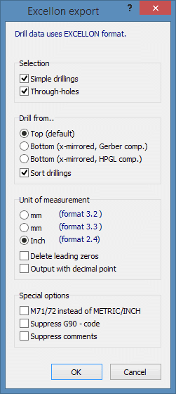
Export Drill data
Please leave the default settings and choose format as 2.4 inches, which includes most decimal places.
Checking of Gerberdata

In addition to our free import service for your data, you can also export your own Gerber data. Please use Gerber RS-274X.
Your exported Gerber files can be checked and printed with the freeware Gerbv or GC PREVUE. This allows testing if everything was exported correctly.
Gerbv and GC PREVUE can be found on our download page.


