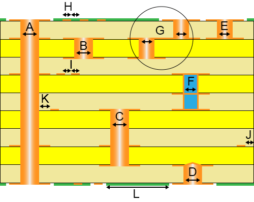
Design Parameters
Here you can download the Basic Design Rules incl. Design Parameters.
The following parameters are exemplary for 35μm copper thickness.
For other thicknesses / special production, please contact our technical hotline: +49 (0)8104 628 210.
| Index | Standard (min.) | Special production(min.) | |||||||
|---|---|---|---|---|---|---|---|---|---|
| Index | A, B, C | Via, buried via Component hole: Annular ring circular + 25µm | aspect ratio diameter via pad annular ring | Standard (min.) | 1:10 200µm 400µm 100µm circular | Special production(min.) | 1:12 150µm 330µm 90µm circular | ||
| Index | D | Blind Via, mechanical max. Ø 300µm | aspect ratio diameter via pad annular ring | Standard (min.) | 1:1 200µm 400µm 100µm circular | Special production(min.) | 1:1.2 150µm 350µm 100µm circular | ||
| Index | E | Blind Via, laser | aspect ratio diameter via pad annular ring | Standard (min.) | - - - - | Special production(min.) | 1:1 100µm 280µm 90µm circular* | ||
| Index | F | Stacked Vias Disproportional high effort. Please contact our CAM department for alternatives. | aspect ratio diameter via pad annular ring | Standard (min.) | - - - - | Special production(min.) | - - - - | ||
| Index | G | Staggered Vias | aspect ratio diameter via pad annular ring | Standard (min.) | 1:1 - 1:12 ** 200µm 400µm 100µm circular | Special production(min.) | 1:1 - 1:12 ** 100µm 300µm 90µm circular | ||
| Index | H, I | Conductors (see Conductor/copper thickness ) | width space | Standard (min.) | 100µm 100µm | Special production(min.) | 75µm | 90µm 100µm | 90µm | ||
| Index | J | Conductor/pad to milling edge Conductor/pad to scoring edge | space | Standard (min.) | 200µm 500µm | Special production(min.) | 200µm 500µm | ||
| Index | K | Conductor/pad to hole (PTH, NPTH) | space | Standard (min.) | 200µm | Special production(min.) | 200µm | ||
| Index | L | Solder-stop, green | clearance bridge | Standard (min.) | 50µm circular 100µm | Special production(min.) | 25µm circ. (BGA) 80µm | ||
| Index | Solder-stop, other colors | clearance bridge | Standard (min.) | - - | Special production(min.) | 50µm circular 125µm |
* Prior data check necessary. ** see Buried Via, Blind Via


