You should pay special attention to solder-stop bridges (solder-stop between two pads or vias), which should not be smaller than 100µm (green solder-stop) or 150µm (coloured solder-stop) respectively.
We can only conditionally recommend vias (vias) covered with solder-stop.
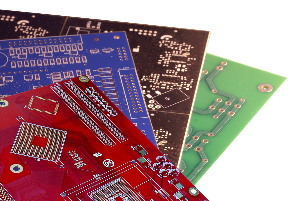
Please refer to our Design Aid Via Covering.
Solder-stop parameters (colour: green)
| clearance min | clearance recommended | bridge width min. | bridge width recommended | |
|---|---|---|---|---|
| Via | 50µm | - | 100µm | 125µm |
| Component hole | 50µm | 75µm | 100µm | 125µm |
| SMD pad | 50µm | 75µm | 100µm | 125µm |
| BGA | 50µm | - | 80µm | - |
Solder-stop parameters (red, blue, white, black, yellow)
| clearance min. | clearance recommended | bridge width min. | bridge width recommended | |
|---|---|---|---|---|
| Via | 50µm | 75µm | 125µm | 150µm |
| Component hole | 50µm | 75µm | 125µm | 150µm |
| SMD Pad | 50µm | 75µm | 125µm | 150µm |
Solder-stop type
Depending on the production line and utilization, we are usinge various brands and processes for the solder-stop. These brands behave technically absolutely equivalent but can slightly differ optical (e.g. matt/glossy).
If a particular solder-stop accomplishment is desired, this may impact costs and production times. The feasibility of certain brand and process -combinations can not always be guaranteed.
Gang mask opening
If the minimum values for solder-stop clearance (50μm) and solder-stop bridge (100μm) are undercut, the complete solder-stop bridge is omitted (so-called gang mask opening). This is done automatically during the Design Rule Check of your production data.
Your advantage through block exemption: Solder-stop bridges < 100μm can peel off, contaminate pads and thus make soldering more difficult. See also Pitch vs. Pad width.
Clearance of component holes

For component holes, please ensure a clearance (spacing between copper to solder-stop) of at least 50µm (green solder-stop).
This clearance should be larger if possible (75µm), to avoid manufacture with extreme tolerances.
For other colours, the minimum solder-stop clearance is 75µm.
The smallest possible solder-stop bridge width is 100µm (green) or 150µm (other colours), respectively.
Clearance of SMD pads (fine pitch)

The minimum solder-stop clearance for SMD pads should at least be 50µm, better: 75µm.
For other colours than green, the min. solder-stop clearance is 75µm.
The smallest possible solder-stop bridge width is 100µm (green) or 125µm (other colours), respectively.
The resulting min. spacing of copper ege to copper edge is 200µm.
BGA (Ball Grid Array)

The following possibilities exist for BGAs (for explanation see Via Covering):
- Via Tenting
- Via Filling
- Via-in-Pad
You should consult your assembly partner when selecting an appropriate surface, normally our customers select the PCB surface finish chemical gold.
Continue with: BGA - Design Recommendations
Pitch vs. Pad width
If the minimum values for solder-stop clearance (50μm) and solder-stop bridge (100μm) are undercut, the complete solder-stop bridge is omitted (so-called gang mask opening or block exemption). Please contact us for a technical solution.
The following is the maximum pad width at a given pitch to get a solder-stop bridge.
Possible solder-stop bridge
| Pad width | 150µm | 200µm | 250µm | 300µm | 400µm | 500µm | 600µm |
|---|---|---|---|---|---|---|---|
| Pitch 0.3 | (✔)* | x | x | x | x | x | x |
| Pitch 0.4 | ✔ | ✔ | (✔)* | x | x | x | x |
| Pitch 0.5 | ✔ | ✔ | ✔ | ✔ | x | x | x |
| Pitch 0.6 | ✔ | ✔ | ✔ | ✔ | ✔ | x | x |
| Pitch 0.7 | ✔ | ✔ | ✔ | ✔ | ✔ | ✔ | x |
| Pitch 0.8 | ✔ | ✔ | ✔ | ✔ | ✔ | ✔ | ✔ |