Finishing treatment

SMD-Schablone Laser

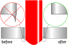
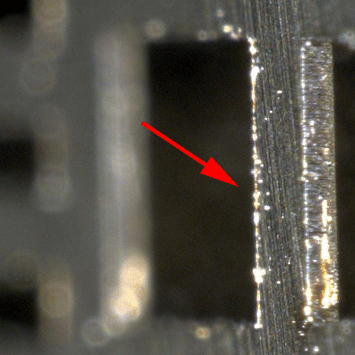
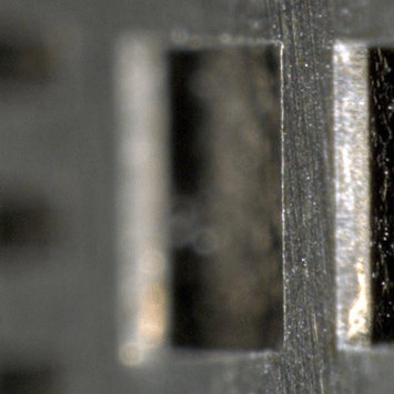
Through the laser cutting process, fine ridges are formed on the pads, which are standardly removed in production by machined deburring (by brushing). The SMD stencils, treated in this way, meet the highest standards.

Using Electropolishing and Nano coating (also Nano protection), the stencil surface can be further improved (optional). This enhances the release behavior of the solder paste and facilitates cleaning of the SMD-Stencil.

For very thin stencils, or for special tension frames, we also offer Edge protection.

Available finishing treatments:

  • Machined deburring two-sided (inclusive)
  • Electropolishing
  • Nano coating
  • Edge protection

Calculate & Order your SMD-Stencil now

Finishing treatment machined deburring

Even for state-of-the-art laser technology, the laser cutting of steel inevitably leads to the smallest burrs, which must be removed before professional assembly. Double-sided brushing removes these burrs.

At Multi-CB, double-sided machined deburring is always included!

Deburring leads to regular paste distribution, higher squeegee life and longer cleaning cycles. 

  • Deburring helps to avoid solder bridges
  • Deburring avoids time-consuming reworking
  • Deburring prolongs the cleaning cycle
  • Deburring improves the release behavior of the solder paste

Example for brushed SMD-Stencils

SMD-Stencil without brushing

without brushing

SMD-Stencil with brushing

with brushing (Multi-CB standard)


Electropolish

SMD pad opening before - after

SMD pad opening before - after

Just for assembly of challenging circuit boards with a high component density, e.g. for components such as μBGAs, 0201 or 01005 as for microelectronics or medical technology, it may be necessary to additionally optimize the surface quality of the SMD-Stencils after laser processing.

Electropolishing, also called Electrochemical surface treatment or Electrochemical deburring, is the solution.

The edges of the SMD pads are deburred and the surface roughness of the inside walls of the pad are smoothed to <1µm (previously <3µm). Thus, the highest demands on surface quality are achievable, a sharp-contoured print is possible in which paste or glue dissolve more easily from the pad opening. The SMD-Stencil is even easier and faster to clean.

Electropolishing is carried out by an acid rinse with additional applied voltage, to control the cutting of roughness. It strikes the aperture walls and the bottom of the stencil. The process is in itself an inverted galvanizing, where metal ions are dispensed in the acid bath.


Nano coating / Nano protection

Nano coating of SMD-Stencil

Through Nano coating, which can be done in addition to Electropolishing, the release behavior of solder paste is once more  optimized.

A drying of solder paste residues is reduced, thereby improving the starting performance after short line shutdowns. In addition, the cleaning efficiency is increased and the cleaning intervals are extended.

Especially for critical, very small pad openings, Nano coating is recommended.

The Nano coating, which is applied only on one side (BOT) has a thickness <5nm and is absolutely REACH compliant.

Example for Nano coated SMD-Stencil in PCB assembly:

without Nano coating after 14 prints

SMD-Stencil without Nano coating - dirty

with Nano coating after 40 prints

SMD-Stencil with Nano coating - clean


Edge protection

Edge protection for SMD-Stencil

On request we can provide your SMD-Stencil with a circumferential Edge protection. This is particularly recommended for very thin stencils for quick-release systems. For this purpose, the edges of the stencil are crimped.

The Edge protection prevents potential cuts from sharp edges and strengthens the outer edges. The metal stencil is more stable and the insertion in a tenter frame is facilitated.

If you wish your SMD stencil manufactured with edge protection, please choose that option in the online calculator. Edge protection is only possible up to a maximum stencil size of 595mm x 595mm.