Please keep in mind the following Design-Rules for your Flex- or Rigid-Flex circuit boards.
For designers of flexible circuit boards we recommend the IPC-2223 Guideline / Design guidelines for flexible circuit boards, which is available at the IPC online store or in German, at the FED website.
General Design Rules for flexible PCBs
If possible, limit the number of flex layers to 1 or 2, for maximum mechanical flexibility and cost savings.
Pay attention to a symmetrical stack-up of the printed circuit board.
The flex layers continue within the rigid part as inner layers and can there be used for conductor routing.
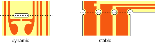
Distinguish between dynamic (regular) and stable flexion (bend-to-install).
The minimum bending radius is usually between 1mm and 5mm. The dynamic bending stress can only be reliably ensured with single- and double-layer flexible printed circuit boards.
Dynamic Bend
Semi-Dynamic
Stable Bend
Bending
Dynamic Bend
frequent
Semi-Dynamic
max. 20x
Stable Bend
„Bend-to-Install“
Layers
Dynamic Bend
1-2L recommended
Semi-Dynamic
1-4L recommended
Stable Bend
1-10L possible
Covering*
Dynamic Bend
PI Coverlay
Semi-Dynamic
PI Coverlay or solder-stop
Stable Bend
PI Coverlay or solder-stop
Min. bending radius
Dynamic Bend
100-150 x h flex
Semi-Dynamic
> 20x h flex
Stable Bend
10 - 20 x h flex
Copper type**
Dynamic Bend
RA copper
Semi-Dynamic
ED or RA copper
Stable Bend
ED or RA copper
h = height
* Flexible solde-stop may break or peel off after 5-10x bending
** RA = Rolled copper, suitable for dynamic, flexible applications; ED = Electrolytically deposited copper , only suited for stable and semi-dynamic applications
Construction examples for flexible PCBs
Layout guidelines
Make track-width and –spacing within the flexible part as wide as possible
At best, the transitions from wide to narrow tracks are continually rejuvenated
From 2 flex layers, shifted placement of tracks on the PCB top and bottom
Make soldering surfaces and annular rings as large as possible
Make connections of tracks and solder pads in a tear-drop, rounded style
Stiffeners (partial mechanical reinforcements, for example, in the plug-in or mounting area) can achieve final thicknesses of 0.2 mm - 1 mm
Flex
< 4 layers
4-6 layers
7-8 layers
min. distance copper - contour
< 4 layers
200µm
4-6 layers
200µm
7-8 layers
200µm
min. distance via - copper
< 4 layers
150µm
4-6 layers
200µm
7-8 layers
300µm
Rigid-Flex
Scope
Minimum
Scope
Flex area length
Minimum
4mm
Scope
Distance PTH (Via) <> Flex area
Minimum
1.5mm
Scope
Distance NPTH <> Flex area
Minimum
0.5mm
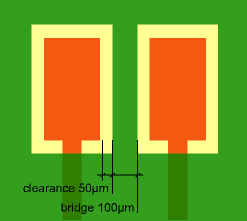
Covering of flexible PCBs
Depending on the application, solder-stop or polyimide (PI) coverlay is recommended as a cover for the flexible circuit board. At best, the maximum possible values for bridge and clearance are used.
PI Coverlay
Solder-stop
Min. bridge
PI Coverlay
350µm
Solder-stop
100µm
Min. clearance
PI Coverlay
200µm
Solder-stop
50µm
Color
PI Coverlay
amber
Solder-stop
green
Application
PI Coverlay
dynamic, stable
Solder-stop
semi-dynamic, stable
PI Coverlay
Solder-stop
Coverlay is not recommended for QFP components unless they are completely exposed!
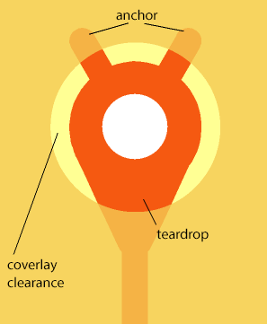
Pads and Vias on flexible PCBs
In general, the copper adhesion in flexible circuit boards is worse than in circuit boards with standard FR4 material. It is therefore recommended to make the pads / annular rings as large as possible. To improve adhesion, anchors and teardrops can be used.
In order to increase the stability of vias on flexible circuit boards, you can implement the following measures:
Give anular rings the maximum size
Bind vias using teardrops
Use anchors to increase the film adhesion
Do not place any vias in the bending area
Calculation of the bending radius
The minimum bending radius r results from the desired application (stable/dynamic) and h, the overall height of the flexible part.
Bending radius acc. to IPC-2223
Stable
Dynamic
1L
Stable
10:1
Dynamic
100:1
2L
Stable
10:1
Dynamic
150:1
ML
Stable
20:1
Dynamic
not recommended*
*The dynamic bending can only be reliably ensured with single- and double-layer flexible printed circuit boards.
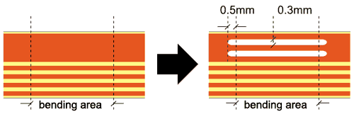
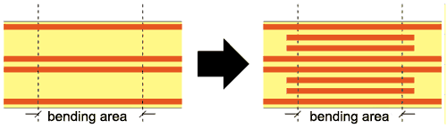
The bending area should have parallel, equal-width tracks with the same insulation resistance which are perpendicular to the bending line.
Divide wide conductor traces into narrower conductor traces within the bending area.
Fill open regions in the bending area with blind conductors.
Ensure a perpendicular path of the conductor traces to the bending axis. Avoid pads plated-through holes in the bending area.
The bending area may be optimized depending on the application.
Dynamic bending: spontaneous and frequent bending Optimization for dynamic bending:
drill holes or slots
copper edges at the bending location
copper stiffeners as bending aids
Stable bending: single occurrence bending, e.g. "bend-to-install" Optimization for stable bends:
drill holes or slots
Contour narrowing
Stabilization through more copper
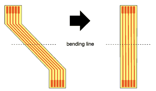
For 2 or more flex layers, please ensure a shifted placement of the conductor traces on the front and back sides of the flexible portion.
Use curves instead of corners in the conductor trace path.
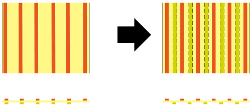
Ground plane
Continuous ground planes in circuit boards should always be rastered due to the copper balance. This also applies to flexible circuit boards. Especially in the flexible bending area, ground planes have to be rastered, since otherwise they break.
Multi-CB can partially apply double-sided ultra-high-temperature adhesive tape from 3M to the Flex and Rigid-Flex PCBs. This allows for easy mounting during final installation. Please use an extra layer in your data for the desired position(s).
Flexible PCBs with 3M adhesive tape can be easily used in the lead-free soldering process (peak temperature 260°C, 20 sec.). The protective cover remains largely undamaged and can be easily removed. The low outgassing of the adhesive reduces the contamination of electronic components.
Technical properties
Product
3M 9077 tape
Product
Adhesive
3M 9077 tape
0,05mm double-coated ultra high temperature acrylic adhesive
Because of the high moisture absorption of polyimide, flexible circuit boards must be dried (approx. 4 h at 120 ° C) prior to the placement and soldering process and processed within 8 hours!
The soldering parameters known from rigid circuit boards can usually be used.
No guarantee! Please always clarify the final parameters with your assembly partner!

![[Translate to English:] Befestigungsmaterial Doppelseitiges Klebeband 3M für Flexible Leiterplatten](https://www.multi-circuit-boards.eu/fileadmin/img/03_Design-Hilfe/flexible%20leiterplatten/3m_9077_flex-befestigung.jpg)