Layer buildup for PCBs
Multilayer circuit boards comprise outer and inner layers (copper layers) and help to achieve more complex, denser wiring structures.
Multilayer circuit boards are pressed from the following components:
- Copper foil
- Prepreg (glass/resin)
- Core (prepreg between 2 copper foils precompressed)
Prepregs and cores are also available as high-Tg and halogen-free versions.
Mixed Dielectric Multilayers (combination of different materials) are possible, please contact us.
Rules for layer buildup
Please observe the following rules for the design of the layer buildup:
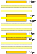
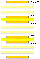
1) Keep the number of prepregs low
Use at most 2 prepregs per layer (also recommended by IPC).
Exceptions with only 1 prepreg: Many layers in a multilayer with defined total thickness, use of microvias (aspect ratio).
Exceptions with 3 and more prepregs include (for example) large thickness of the copper foil on the cores.
Advantages:
- Improved dimensional stability
- Reduced costs
- Reduces thickness tolerance
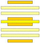
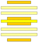
2) Identical copper thickness on the cores
Always plan the cores with identical copper cladding.
Advantages:
- Less bowing, twisting, or deformation
- Symmetric design
- Reduced under etchingg
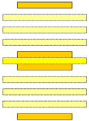
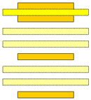
3) Symmetric layer buildup
Ensure a uniform distribution of the 3 components: prepreg, core, and copper foil
Advantages:
- Less bowing, twisting, or deformation
- Reduced costs
- Improved process reliability
SBU-Multilayer
Multi-CB can also create sequential layer buildups (= SBU), in which multiple pressure sequences are used. This permits use of blind vias and buried vias, allowing even higher integration levels.
For SBU multilayers, the circuitry is divided in a bi- or multilayer core and one or multiple external microvia layers (vias with diameter smaller than 150µm).
Lasered blind vias
Blind vias are lasered for diameters smaller than 150µm. The prepreg and copper foil are then replaced by RCC (Resin Coated Copper) foil, whose resin is similar to the epoxy in FR4.
Electric strength
To maintain the highest possible capacitance between two large-area potentials, the layer spacing should be as small as possible. The necessary voltage separation between the potential and bordering layers require a minimum thickness. The following value may be used to calculate the optimum spacing:
The electric strength of FR4 is approx. 30 kV/mm.