Plated Half-holes
Plated half-holes (or castellated holes) are predominantly used for board-on-board connections, mostly where two printed circuit boards with different technologies are combined. E.g. the combination of complex microcontroler modules with common, individually designed PCBs.
Additional applications are display, HF or ceramic modules which are soldered to the base printed circuit board.
The board-on-board PCBs therefore need plated half-holes, which serve as SMD connection pads. Through directly connecting the PCBs together, the whole system is considerably thinner than a comparable connection with multi-pin connectors.
Advice
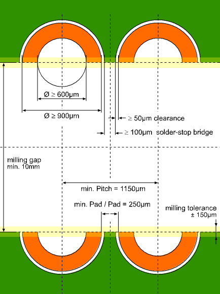
- The milling tolerance is +/- 150µm
- Distance pad to pad: min. 250µm
- The milling gap within a panel needs to be 10mm min. (see drawing)
- Use the largest hole diameter possible
- Use the largest outerlayer pad possible, both top and bottom sides
- If possible, connect innerlayer pads to the plated hole (brings more stability and helps to avoid burrs)
Manufacturing
Through setting back the copper shell from the conture, the plating is protected from mechanical damaging.
Therefore the plated half-holes can be milled precisely what strongly improves the process reliability.
Internal Half-holes are also producable.


Design Parameters
The following table contains the minimum parameters!
| Ø drill | Ø pad | pad / pad | clearance | solder-stop bridge | pitch min. | ||||||
|---|---|---|---|---|---|---|---|---|---|---|---|
| Ø drill | 600µm | Ø pad | 900µm | pad / pad | 250µm | clearance | 50µm-75µm | solder-stop bridge | 100µm | pitch min. | 1150µm |
Drawing