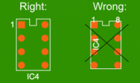
The spacing between solder pad and marking print should be at least 150µm.
Always avoid overprinting solder pads!
A marking print is helpful for error-free manual assembly, but also for including a revision number or UL-number on the circuit board. Multi-CB can provide marking prints in the colours white, yellow, and black.
Solder pads should never be overprinted, because this may lead to problems during soldering, assembly, and with the E-Test. If we should detect an overprinted solder pad (spacing < 150µm), then Multi-CB reserves the right to remove the marking print at this location. Relevant for the definition of the solder pads is the solder pad exemption. The marking print is usually automatically clipped with a spacing of 100µm to the solder-stop edge.
Min. spacing to pads | 150µm |
---|
Font height | Optimum font width | ||
---|---|---|---|
Font height | 1,2mm | Optimum font width | 150µm (6mil) |
Font height | 1,8mm | Optimum font width | 200µm (8mil) |
Proposal for placement of marking print.
The spacing between solder pad and marking print should be at least 150µm.
Always avoid overprinting solder pads!
Before exporting your data, you should always activate the option "Always vector font", which is found under: Options / User interface. Otherwise your marking print will very probably be incorrectly applied (see EAGLE 5-Manual, page 44).